

“つなぐ”を変えれば、デバイスの未来が変わる。
スマートフォン、ロボット、ウェアラブルセンサ、宇宙機器。
あらゆる電子デバイスの中には、材料と材料、部品と部品を「つなぐ」技術があります。
当研究室では、この「接合」に着目し、界面改質技術を用いて、接着剤やはんだを使わずに様々な材料を直接つなぐ新しい接合法を開発しています。
接続部から接着剤・はんだをなくすことで、デバイスの薄型化・高信頼化・高耐久化・高性能化が可能になります。
さらに、開発した技術をロボット、フレキシブルエレクトロニクス、ヘルスケアデバイス、宇宙用デバイスへ応用し、基礎技術から実デバイスまで一貫してつくり込む研究を進めていきます。
2026年に発足した若い研究室だからこそ、学生一人ひとりが研究室の文化と研究テーマを一緒につくっていくことができます。
(English version below)
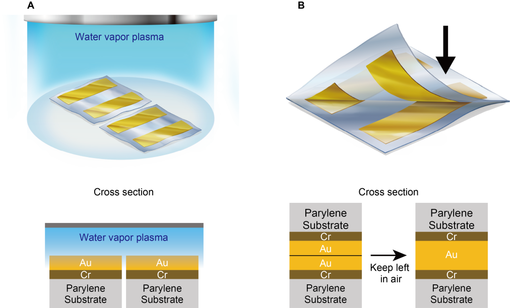
素材は、空気中に放置すればゴミで表面が覆われます。しかし、適切にそのゴミを除去して、表面を極限まできれいにしたら何が起こるでしょうか。
例えば、金属だったら、溶かさず接触させるだけで原子レベルの強固な接合が生じます。
じゃぁ、直接接合を配線の接続法として応用したら、、、
極低接触抵抗、極柔軟特性など新たな価値を発現します。
本研究室では、特に直接接合法で「ペラペラの柔らかな電子素子」を柔らかく接続する、世界初の技術を有しています。
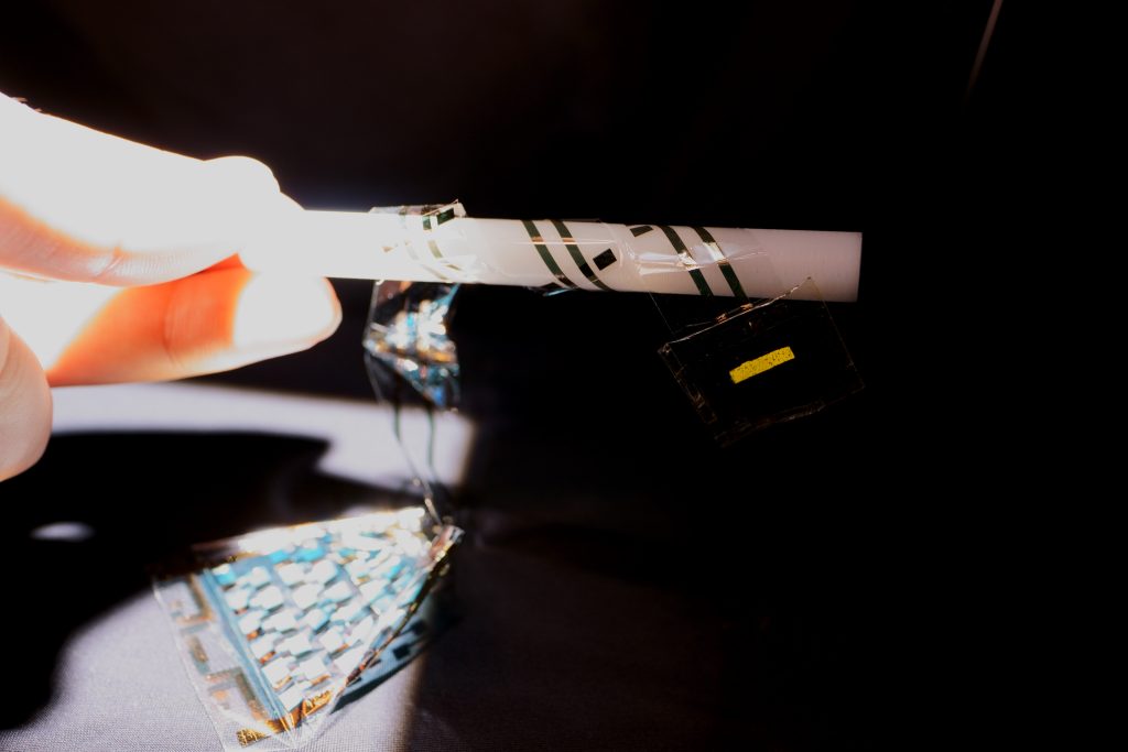
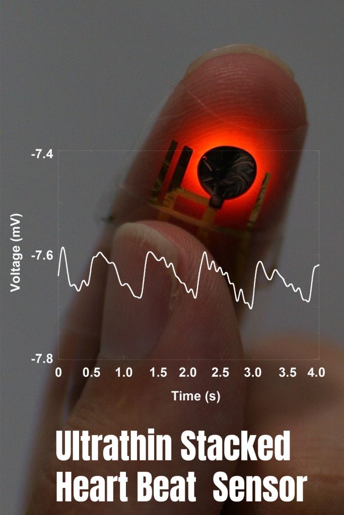
直接接合法を柔軟実装法として応用することで、柔軟性を保ちながら素子を3D集積化させる事が可能になります。
これは、従来の接着剤接合における柔軟性と積層数のトレードオフを打破する、本手法の優位性です。
この研究では、有機LEDと有機OPDを積層実装し、脈拍の測定に成功しました。
(doi:10.1002/adma.202417590)
What happens when a surface becomes truly clean?
Materials exposed to air are quickly covered by contaminants.
However, if these contaminants are carefully removed and the surface is cleaned to the limit, something remarkable can happen.
For example, when two clean metal surfaces are brought into contact, they can form a strong atomic-level bond — without melting, adhesives, or solder.
This is the starting point of our research: controlling surfaces and interfaces to create new ways of joining materials.
What if direct bonding is applied to electrical interconnections?
Direct bonding is not only a way to join materials.
When applied to electrical interconnections, it can create new value, such as ultralow contact resistance, exceptional flexibility, and highly reliable device integration.
Our laboratory has developed a pioneering technology that uses direct bonding to softly connect ultrathin, flexible electronic devices — without adhesives or solder.
This enables the creation of next-generation electronics that are not only thin and lightweight, but also mechanically robust, electrically reliable, and truly flexible.
Toward 3D integration of truly flexible electronics
By applying direct bonding as a flexible integration technology, electronic components can be stacked in three dimensions while maintaining their softness and flexibility.
This is a key advantage of our approach: it overcomes the conventional trade-off between flexibility and the number of stacked layers, which has been a major limitation in adhesive-based integration.
In this study, we demonstrated the stacked integration of an organic light-emitting diode and an organic photodetector, and successfully measured pulse waves using the integrated device.
(doi:10.1002/adma.202417590)